- 您现在的位置:买卖IC网 > Sheet目录318 > CAT3606HV4-T2 (ON Semiconductor)IC LED DRVR WHITE BCKLGT 16-TQFN
CAT3606
TYPICAL CHARACTERISTICS
(V IN = 3.6 V, EN = V IN , ENM = ENS = GND, C IN = C OUT = 1 m F, T AMB = 25 ° C, unless otherwise specified.)
5
4
1.24
1.22
1x Mode
3
1.20
2
1
1.18
0
0
100
200
300
400
500
1.16
? 50
? 25
0
25
50
75
100
125
OUTPUT CURRENT (mA)
Figure 21. Foldback Current Limiting
TEMPERATURE ( ° C)
Figure 22. RSET Pin Voltage vs. Temperature
ENM & ENS
5V/div
VOUT
1V/div
Tot. LED
Current
50mA/div
200 m sec/div
Figure 23. PWM Dimming at 1 kHz on ENM and ENS
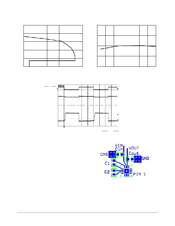
Recommended Layout
When the driver is in the 1.5x charge pump mode, the
1 MHz switching frequency operation requires to minimize
trace length and impedance to ground on all 4 capacitors. A
ground plane should cover the area on the bottom side of the
PCB opposite to the IC and the bypass capacitors.
Capacitors Cin and Cout require short connection to ground
which can be done with multiple vias as shown on Figure 24.
A square copper area matches the QFN16 exposed pad
(GND) and must be connected to the ground plane
underneath. The use of multiple via will improve the heat
dissipation.
http://onsemi.com
9
Figure 24. PCB Layout
发布紧急采购,3分钟左右您将得到回复。
相关PDF资料
CAT3614HV2-T2
IC LED DRVR WHITE BCKLGT 12-TDFN
CAT3616HV4-GT2
IC LED DRVR WHITE BCKLGT 16-TQFN
CAT3636HV3-GT2
IC LED DVR 6CH QUAD MODE 16TQFN
CAT3643HV2-T2
IC LED DRVR WHITE BCKLGT 12-TDFN
CAT3644HV3-GT2
IC LED DVR 4CH QUAD MODE 16TQFN
CAT3647HV3-GT2
IC LED DRVR WHITE BCKLGT 16-TQFN
CAT3648HV3-GT2
IC LED DRVR WHITE BCKLGT 16-TQFN
CAT3661HV3-GT2
IC LED DRVR WHT BCKLGHT 16TQFN
相关代理商/技术参数
CAT3612
制造商:CATALYST 制造商全称:Catalyst Semiconductor 功能描述:Programmable 300mA Camera Flash LED Driver
CAT3612_08
制造商:CATALYST 制造商全称:Catalyst Semiconductor 功能描述:Programmable 300mA Camera Flash LED Driver
CAT3612HV2-GT2
功能描述:LED照明驱动器 LED Driver,Charge pump,2 ch RoHS:否 制造商:STMicroelectronics 输入电压:11.5 V to 23 V 工作频率: 最大电源电流:1.7 mA 输出电流: 最大工作温度: 安装风格:SMD/SMT 封装 / 箱体:SO-16N
CAT3612HV2-T2
功能描述:LED照明驱动器 Prog Camera Flash LED Driver RoHS:否 制造商:STMicroelectronics 输入电压:11.5 V to 23 V 工作频率: 最大电源电流:1.7 mA 输出电流: 最大工作温度: 安装风格:SMD/SMT 封装 / 箱体:SO-16N
CAT3614
制造商:CATALYST 制造商全称:Catalyst Semiconductor 功能描述:4-Channel 1-Wire LED Driver in 3x3mm Package
CAT3614_08
制造商:CATALYST 制造商全称:Catalyst Semiconductor 功能描述:4-Channel 1-Wire LED Driver in 3 x 3mm Package
CAT3614HS2-T2
制造商:CATALYST 制造商全称:Catalyst Semiconductor 功能描述:4-Channel 1-Wire LED Driver in 3x3mm Package
CAT3614HV2-GT2
功能描述:LED照明驱动器 LED Driver,Charge pump,4 ch RoHS:否 制造商:STMicroelectronics 输入电压:11.5 V to 23 V 工作频率: 最大电源电流:1.7 mA 输出电流: 最大工作温度: 安装风格:SMD/SMT 封装 / 箱体:SO-16N
